- Home
- Product
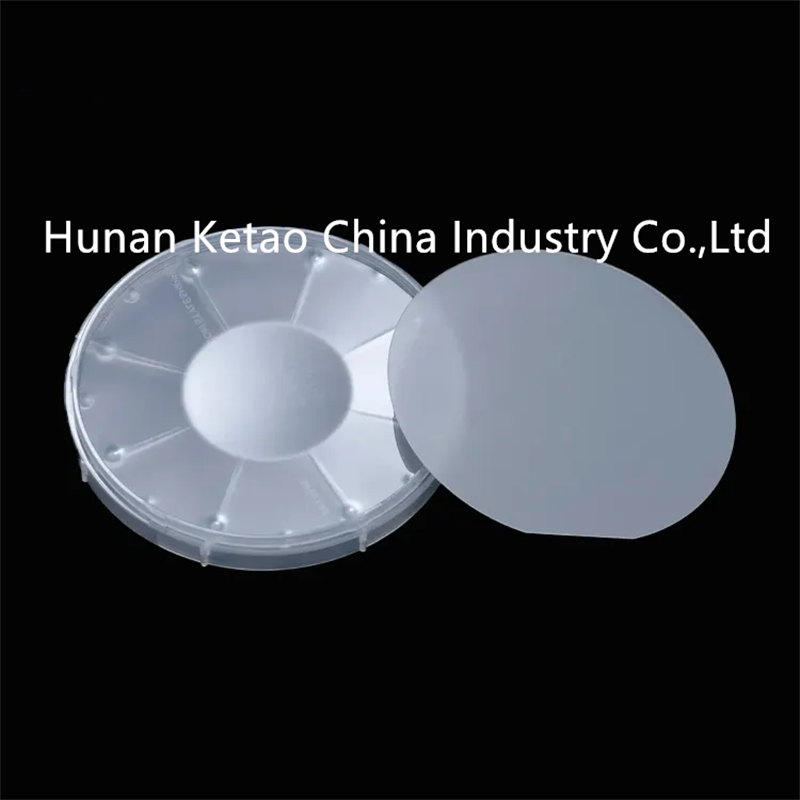
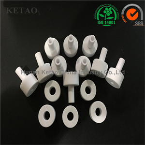
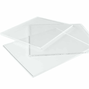
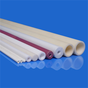
- Alumina Ceramics
- Alumina Ceramic Tube Alumina Ceramic Rod Alumina Ceramic Substrates Alumina Ceramic Disc Alumina Ceramic Plate Alumina Ceramic Roller Alumina Ceramic Crucible Alumina Ceramic Ring Alumina Ceramic Part Ceramic Ignition Electrode series
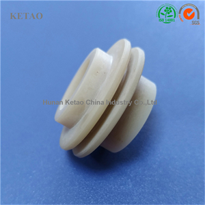
- Zirconia Ceramics
- Zirconia Ceramic Tube Zirconia Ceramic Rod Zirconia Ceramic Plate Zirconia Ceramic Disc Zirconia Ceramic Crucible Zirconia Ceramic Ring Zirconia Part Zirconia Knife
- Aluminum Nitride Ceramics
- Aluminum Nitride Substrates Aluminum Nitride Tube Aluminum Nitride Plate Aluminum Nitride Disc Aluminum Nitride Part
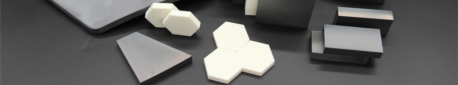
- Boron Carbide Ceramics
- Boron Carbide Tiles Boron Carbide Plate Boron Carbide Insert Boron Carbide Bushing Boron Carbide Tube Boron Carbide Nozzle Boron Carbide Ball
- Boron Nitride Ceramics (BN)
- Boron Nitride Tube Boron Nitride Plate Boron Nitride Ring Boron Nitride Nozzle Boron Nitride Crucible Boron Nitride Part
- Silicon Nitride (Si3N4) Ceramics
- Silicon Nitride Substrates Silicon Nitride Bearing Silicon Nitride Igniter Silicon Nitride Balls Silicon Nitride Tube Silicon Nitride Part
- About Us
- News
- Contact Us